Che cos'è un dispositivo sensibile alle scariche elettrostatiche?
I dispositivi sensibili alle scariche elettrostatiche (ESD) si riferiscono a componenti elettronici vulnerabili ai danni da scarica elettrostatica (ESD). Questi dispositivi possono essere danneggiati da improvvisi picchi di tensione causati dall'elettricità statica. Anche scariche di bassa energia (ad esempio, poche centinaia di volt) possono degradare le prestazioni o causare un guasto immediato.
Quali dispositivi sono sensibili alle scariche elettrostatiche?
I comuni dispositivi sensibili alle ESD includono:
- Circuiti integrati (IC): Microprocessori, chip di memoria (ad esempio, RAM, Flash) e porte logiche (ad esempio, CMOS, TTL).
- Transistor: MOSFET (transistor a effetto di campo a semiconduttore metallico) e BJT (transistor a giunzione bipolare).
- Diodi: LED (Light-Emitting Diodes) e diodi laser.
- Sensori di precisione: Sensori di immagine (ad esempio, CCD, CMOS) e sensori MEMS (Micro-Electro-Mechanical Systems).
- Componenti analogici: Amplificatori operazionali (Op-Amp) e regolatori di tensione.
- Semiconduttori discreti: Tiristori e IGBT (Transistor bipolari a porta isolata).
- Componenti passivi con caratteristiche avanzate: Resistenze a film sottile e condensatori ad alta frequenza.
Questi dispositivi sono altamente suscettibili di essere danneggiati dalle scariche elettrostatiche (ESD) a causa delle loro piccole e delicate strutture interne.
In che modo i dispositivi sensibili alle ESD possono essere danneggiati dalle ESD?

L'ESD danneggia i dispositivi sensibili attraverso impulsi di alta tensione/corrente generati durante la scarica elettrostatica. I meccanismi chiave includono:
- Sovraccarico termico: Il rapido trasferimento di energia fonde o vaporizza piccoli percorsi conduttivi (ad esempio, le giunzioni dei transistor), causando un guasto permanente.
- Ripartizione dell'isolamento: L'alta tensione perfora sottili strati dielettrici (ad esempio, gli ossidi di gate dei MOSFET), creando cortocircuiti o perdite.
- Iniezione di carica: Le cariche statiche alterano le proprietà dei semiconduttori, degradando le prestazioni (ad esempio, le soglie spostate nella logica CMOS).
- Difetti latenti: I danni parziali possono indebolire i componenti e causare guasti prematuri durante il funzionamento.
Anche le scariche a bassa energia (ad esempio, <100V) possono danneggiare la moderna elettronica su scala nanometrica.
Quando si trasportano dispositivi sensibili alle scariche elettrostatiche da una struttura all'altra, utilizzare?
Per trasportare e conservare in modo sicuro i dispositivi sensibili alle scariche elettrostatiche, utilizzare sacchetti con schermatura statica, schiuma conduttiva o contenitori a prova di ESD con messa a terra. Mantenere il controllo dell'umidità, evitare lo stress fisico ed etichettare le confezioni per garantire la conformità agli standard ESD, come ad esempio ANSI/ESD S541 & IEC-61340-5-3-2022 .
Qual è la tensione minima di scarica elettrostatica (ESD) che può danneggiare i dispositivi sensibili alle scariche elettrostatiche?
I dispositivi sensibili alle scariche elettrostatiche possono subire danni da tensioni fino a 20 volt, impercettibili per l'uomo. I componenti avanzati, come i circuiti integrati o i MOSFET, sono vulnerabili anche a livelli inferiori.
Come gestire i dispositivi sensibili alle scariche elettrostatiche?
La manipolazione di dispositivi sensibili alle scariche elettrostatiche richiede una comprensione completa dei materiali con cui si lavora, in particolare della loro vulnerabilità alle scariche elettrostatiche (ESD). Un'operazione di successo Programma di controllo ESD si basa sull'identificazione dei dispositivi più sensibili alle ESD e sulla valutazione dei loro livelli di suscettibilità. A tal fine è necessario familiarizzare con i Modello del corpo umano (HBM) e il Modello di dispositivo caricato (CDM) sensibilità di tutte le apparecchiature presenti nella vostra struttura.
Modello del corpo umano (HBM)
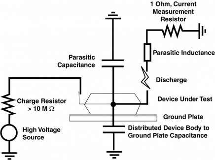
Una delle cause più comuni di eventi ESD è il trasferimento diretto di cariche elettrostatiche dal corpo umano al dispositivo ESDS. Il Modello del corpo umano (HBM) imita questo scenario simulando il flusso di scariche elettrostatiche dal polpastrello di un individuo in piedi a un dispositivo. Ecco come funziona:

- Un condensatore da 100 pF viene caricato attraverso un resistore ad alta resistenza (tipicamente nell'ordine dei megaohm) mediante un interruttore.
- La carica immagazzinata si scarica attraverso un resistore da 1.500 ohm collegato in serie al dispositivo di test.
- Il dispositivo viene quindi messo a terra o passa a uno stato di basso potenziale.
Questo metodo, standardizzato in ANSI/ESDA/JEDEC JS-001-2024 (Electrostatic Discharge Sensitivity Testing - Human Body Model), garantisce una valutazione coerente della resistenza di un componente agli eventi ESD provocati dall'uomo.
Modello di dispositivo caricato (CDM)
Un'altra causa importante di danni da ESD è la carica del dispositivo stesso durante i processi di produzione o di manipolazione, che può portare a una rapida scarica quando entra in contatto con una superficie conduttiva a un potenziale inferiore. Il Modello di dispositivo caricato (CDM) riproduce questo fenomeno simulando la rapida scarica della carica statica accumulata da un componente carico a una superficie messa a terra.
Ecco come funziona:
- Fase di carica: Il dispositivo acquisisce carica elettrostatica attraverso l'attrito o il contatto con materiali isolanti (ad esempio, imballaggi, nastri trasportatori), agendo come una piastra di un condensatore. La carica immagazzinata dipende dalla capacità intrinseca del dispositivo (in genere 10-200 pF) e dalle condizioni ambientali.
- Fase di scarico: Quando il pin di un dispositivo carico entra in contatto con un conduttore a terra, l'energia accumulata si scarica bruscamente attraverso il pin. Questa scarica genera correnti di picco estremamente elevate (fino a 20 kA) in pochi nanosecondi, grazie alla minima resistenza e induttanza del percorso.
- Configurazione del test: Il test CDM valuta la resilienza di un dispositivo caricandolo a una tensione definita (ad es. 250-1000 V per ANSI/ESDA/JEDEC JS-002) e innescando la scarica attraverso un percorso a bassa resistenza. L'impostazione del test tiene conto dell'orientamento del dispositivo, del tipo di confezione e della capacità parassita.
10 consigli fondamentali per la gestione dei dispositivi sensibili alle scariche elettrostatiche
La manipolazione di dispositivi sensibili alle scariche elettrostatiche (ESD) richiede un'attenzione particolare per evitare danni. Ecco dieci consigli fondamentali per garantire una manipolazione sicura:

- Utilizzare spazi di lavoro sicuri per le scariche elettrostatiche
Lavorare sempre in un Area protetta da ESD (EPA) dotati di tappetini antistatici & Pavimenti ESD, superfici di lavoro con messa a terra e un'adeguata Simboli ESD. - Indossare un abbigliamento sicuro per le scariche elettrostatiche
Utilizzare un sistema antistatico cinghie da polso, cinghie per il tallonee camici ESD per evitare l'accumulo di cariche elettrostatiche sul corpo. - Mettere a terra se stessi in modo appropriato
Collegare il bracciale antistatico a un punto collegato a terra prima di maneggiare dispositivi sensibili alle scariche elettrostatiche. - Maneggiare i dispositivi per i bordi
Evitare di toccare direttamente pin, connettori o circuiti. Tenere i componenti per i bordi per ridurre al minimo il rischio di ESD. - Utilizzare imballaggi a prova di ESD
Conservare e trasportare i dispositivi sensibili alle scariche elettrostatiche in sacchetti antistatici, schiuma conduttiva o contenitori schermati. - Controllo dei livelli di umidità
Mantenere un'umidità relativa di 30-70% nell'area di lavoro per ridurre l'accumulo di elettricità statica. - Utilizzare gli ionizzatori per la neutralizzazione
Utilizzare ionizzatori per neutralizzare le cariche statiche sulle superfici e sui materiali non conduttivi dell'APE. - Controllo quotidiano dei dispositivi di messa a terra ESD
Utilizzo Tester combinato ESD controllare quotidianamente i sistemi di messa a terra personali, per assicurarsi che funzionino correttamente. - Evitare materiali altamente statici
Tenere plastica, vinile e altri materiali altamente statici lontani dai dispositivi e dalle aree di lavoro sensibili alle scariche elettrostatiche. - Limitare il movimento nell'EPA
Ridurre al minimo i movimenti non necessari nell'APE per ridurre la generazione di elettricità statica causata dall'attrito o dalle correnti d'aria.